

Micro- LED Display Technology
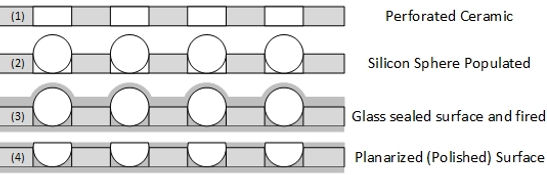

Schematic of example process: (1) A perforated ceramic is filled with (2) previously refined, single crystal semiconductor spheres, (3) conformally coated, and (4) planarized to expose the cross section of the spheres for standard lithography.
4 inch procesed substrate. (1) Holes are made in a Low Temperature Co-fired Ceramic (LTCC) “green tape” substrate, (2) Silicon Spheres are placed in the holes with glass paste, conformally coated and fired, and (3) the assembly is planarized.
MARKET OPPORTUNITY
LED video displays are a $10B market. It is also the last passive-matrix video device in production. The existing process uses discrete LEDs on conventional PCBs. With a passive backplane, all the image artifacts, drive issues and poor video quality that drove passive displays out of existence are preventing LED based displays from entering new markets such as digital cinema, and encroaching on the high-end, large TV market. No active-backplane technology has the required combination of performance, scalability and cost of manufacture.
COMPETITIVE ADVANTAGE
Silicon on Demand is a novel, patented [1]-[3], and low-cost process for printing large numbers of small regions of single-crystal silicon on large area substrates. The process makes use of well-established semiconductor industry technologies. For active backplane micro-LED displays no active-backplane technology exists.
Schematic of example process: (1) A perforated ceramic is filled with (2) previously refined, single crystal semiconductor spheres, (3) conformally coated, and (4) planarized to expose the cross section of the spheres for standard lithography.
Using technology from photo-voltaic solar panels, approximately spherical particles of single-crystal silicon have been manufactured in diameters ~1 mm. The process [4] uses particles of silicon positioned in holes in a ceramic. The assembly is conformally coated and planarized to expose the interior of the sphere. Planarization is a standard technique in integrated circuit manufacture, and is used here in a modified way shown schematically. The result of planarizing the surface is that the internal cross-section of the silicon spheres is exposed. The flat cross section and planar surface allows the use of standard photolithographic device fabrication techniques. Because the spheres are purified in a separate process, high-purity single-crystal material can be realized. A Si process using planarized spheres has been demonstrated with device mobility greater than 300 cm2/V·Sec [5]. This process is being used to design an LED video tile [6] for video wall application.
1. “Planarized semiconductor particles positioned on a substrate, “ D. R. Dykaar, US 9,224,851, (2015).
2. “Method of fabricating crystalline island on substrate, ” D. R. Dykaar, US 20150357192 (2015).
3. “Method and system for manufacturing a semi-conducting backplane, ” D. R. Dykaar, US 9,209,019, (2015).
4. "Large Area Display Backplane Using Embedded Single-Crystal Silicon Particles, " D. R. Dykaar, B. Esfandiarpour, F. Chen, S. Guthrie, G. Hill, J. Vieth and S. Sivoththaman, Society for Information Display Symposium Digest of Technical Papers, 44.4L: Late-News Paper, Volume 45, Issue 1, pgs. 638–641, 2014.
5. “Device Mobility >300 cm2/V·S Using Planarized Single-Crystal Silicon Spheres for Large Area Display Backplanes, ” R. S. Tarighat, F. Chen, G. Hill, J. Vieth, S. Sivoththaman, and D. R. Dykaar, Society for Information Display Symposium Digest of Technical Papers, P-190L: Late-News Poster, 2016.
6. “Active Backplane Design for Digital Video Walls, “ D. R. Dykaar, R. S. Tarighat, F. Chen, T. Davidson-Hall, G. Hill, J. Vieth, C. Brown, H. Aziz, and S. Sivoththaman, Society for Information Display Symposium Digest of Technical Papers, 69-4, 2016.